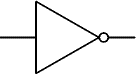
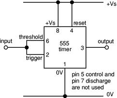
The buffer circuit's input has a very high impedance (about 1MΩ) so it requires only a few µA, but the output can sink or source up to 200mA. This enables a high impedance signal source (such as an LDR) to switch a low impedance output transducer (such as a small lamp).
It is an inverting buffer or NOT gate because the output logic state (low/high) is the inverse of the input state:
Input low (< 1/3 Vs) makes output high, +Vs
Input high (> 2/3 Vs) makes output low, 0V
When the input voltage is between 1/3 and 2/3 Vs the output remains in its present state. This intermediate input region is a deadspace where there is no response, a property called hysteresis, it is like backlash in a mechanical linkage. This type of circuit is called a Schmitt trigger.
If high sensitivity is required the hysteresis is a problem, but in many circuits it is a helpful property. It gives the input a high immunity to noise because once the circuit output has switched high or low the input must change back by at least 1/3 Vs to make the output switch back.
555 inverting buffer circuit (NOT gate)
Rapid Electronics: NE555 timer (standard)
Rapid Electronics: ICM7555 (low power)