
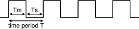
Time period and frequency | Mark/Space times | Duty cycle | PWM | Operation
The 555 timer IC can be used with a few simple components to build an astable circuit which produces a 'square wave'. This is a digital waveform with sharp transitions between low (0V) and high (+Vs), the durations of the low and high states may be different. The circuit is called an astable because it is not stable in any state: the output is continually changing between 'low' and 'high'.
The time period (T) of the square wave is the time for one complete cycle, but it is often better to consider frequency (f) which is the number of cycles per second.
| T = 0.7 × (R1 + 2R2) × C1 |
| f = | 1.4 |
| (R1 + 2R2) × C1 |
T = time period in seconds (s)
f = frequency in hertz (Hz)
R1 = resistance in ohms (Ω)
R2 = resistance in ohms (Ω)
C1 = capacitance in farads (F)
If R1 is much less than R2 we can ignore R1 and use:
| T = 1.4 × R2 × C1 (when R1 << R2) |
555 astable output, a square wave
(Tm and Ts may be different)

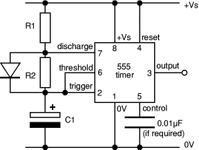
555 astable circuit
A 1 second time period is a good starting value if you are experimenting with flashing LEDs or producing a clock signal for testing counters.
These values give an appoximate 1 second time period:
R1 = 1kΩ, R2 = 68kΩ and C1 = 10µF.
Example breadboard layout for this circuit:

For breadboard projects using a 555 astable circuit see Breadboard Workshop 1.
| Example 555 astable R1, R2 & C1 values for equal on and off times, Tm = Ts | ||||
| Time Period (approx.) | Frequency (approx.) |
R1* | R2 | C1 |
| 10s | 0.1Hz | 1kΩ | 68kΩ | 100µF |
| 3s | 0.3Hz | 1kΩ | 220kΩ | 10µF |
| 2s | 0.5Hz | 1kΩ | 150kΩ | 10µF |
| 1s | 1Hz | 1kΩ | 68kΩ | 10µF |
| 0.3s | 3Hz | 1kΩ | 220kΩ | 1µF |
| 100ms | 10Hz | 1kΩ | 68kΩ | 1µF |
| 20ms | 50Hz | 1kΩ | 150kΩ | 0.1µF |
| 10ms | 100Hz | 1kΩ | 68kΩ | 0.1µF |
| 2ms | 500Hz | 1kΩ | 150kΩ | 0.01µF |
| 1ms | 1kHz | 1kΩ | 68kΩ | 0.01µF |
| 0.3ms | 3kHz | 1kΩ | 22kΩ | 0.01µF |
| * If R2 is 100kΩ or more you can increase
R1 to 10kΩ and still have equal on/off times. | ||||
The time period can be split into two parts:
| Time period, T = Tm + Ts |
| Mark time (output high) Tm = 0.7 × (R1 + R2) × C1 |
| Space time (output low) Ts = 0.7 × R2 × C1 |
It is important to note that Tm must be greater than Ts since R1 cannot be 0Ω (the minimum is 1kΩ).
Many circuits require Tm and Ts to be about equal. This is achieved if R2 is much larger than R1.
For a standard astable circuit note that Tm will always be greater than Ts because Ts is propotional to R2 but Tm is propotional to R2 + R1 and R1 cannot be zero.
This is not too restricting because the output can both sink and source current. For example an LED can be made to flash briefly with long gaps by connecting it (with its resistor) between +Vs and the output. This way the LED is on during Ts, so brief flashes are achieved with R1 larger than R2, making Ts short and Tm long.
If R1 is much less than R2, Tm and Ts will be very similar and that's usually good enough for circuits which need Tm and Ts to be (roughly) equal.
If Tm must be less than Ts a diode can be added to the circuit as explained under duty cycle below.
R1 and R2 should be in the range 1kΩ to 1MΩ. It is best to choose C1 first because capacitors are available in just a few values.
Choose C1 to suit the frequency range you require (use the table as a guide).
Choose R2 to give the frequency (f) you require. Assume that R1 is much smaller than R2 (so that Tm and Ts are almost equal), then you can use:
| If R1 << R2 use | |
| R2 = | 0.7 |
| f × C1 | |
Choose R1 to be about a tenth of R2 (the minimum is 1kΩ) unless you want the mark time Tm to be significantly longer than the space time Ts.
If you need a variable resistor it is best to make it R2.
Beware that if R1 is variable it must have a fixed resistor of at least 1kΩ in series (this is not required for R2).
| 555 astable frequencies | |||
| C1 | R2 10kΩ R1 1kΩ |
R2 100kΩ R1 10kΩ |
R2 1MΩ R1 100kΩ |
| 0.001µF | 68kHz | 6.8kHz | 680Hz |
| 0.01µF | 6.8kHz | 680Hz | 68Hz |
| 0.1µF | 680Hz | 68Hz | 6.8Hz |
| 1µF | 68Hz | 6.8Hz | 0.68Hz |
| 10µF | 6.8Hz | 0.68Hz (41 per min.) | 0.068Hz (4 per min.) |
There is more information about 555 timers and their circuits on the Electronics in Meccano website.
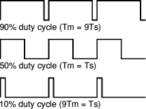
The duty cycle of an astable circuit is the proportion of the complete cycle for which the output is high (the mark time). It is usually given as a percentage.
For a standard 555 astable circuit the mark time (Tm) must be greater than the space time (Ts), so the duty cycle must be at least 50%:
| Duty cycle = | Tm | = | R1 + R2 |
| Tm + Ts | R1 + 2R2 |
To achieve a duty cycle of less than 50% a signal diode (such as 1N4148) can be added in parallel with R2 as shown in the diagram. This bypasses R2 during the charging (mark) part of the cycle so that Tm depends only on R1 and C1:
| 555 astable with diode (for duty cycle < 50%) |
| Tm = 0.7 × R1 × C1 (ignoring 0.7V across diode) |
| Ts = 0.7 × R2 × C1 (unchanged) |
| T = Tm + Ts = 0.7 × (R1 + R2) × C1 |
| Duty cycle with diode | = | Tm | = | R1 |
| Tm + Ts | R1 + R2 |
555 astable circuit with diode across R2
Tm can be less than Ts so the
duty cycle can be less than 50%
Pulse Width Modulation (PWM) is the technique of using the duty cycle (see above) of a digital (on/off) signal to control an analogue quantity such as the brightness of an LED or the speed of a motor.
For example an LED will be bright if the duty cycle is 90% (mostly on), but dim if the duty cycle is 10% (mostly off).
The pulse frequency must be sufficiently high for the output to appear continuous, for example 1kHz (1000 flashes per second) which is too fast for our eyes to see the rapid flashes, instead we see an average brightness determined by the duty cycle.
The circuit diagram shows how 2 diodes and a variable resistor can be used with a 555 timer to make a PWM circuit for varying the brightness of an LED. The diodes ensure that one part of the variable resistor track (plus 1kΩ) is used for the mark time (Tm) while the other part is used for the space time (Ts). This arrangement ensures that the total time period, Tm + Ts, (and frequency) is almost constant while the duty cycle is varied. The 1kΩ resistor ensures that R1 is never less than 1kΩ to protect the 555 timer. With the values shown the frequency is about 1kHz, this is ideal for varying the brightness of an LED.
Use three PWM circuits like this to independently vary the brightness of the red, green and blue LEDs inside an RGB LED to produce a wide range of colours.

If you wish to use a 9V supply (instead of 6V as shown) change the 330Ω LED resistor to 470Ω.
555 astable PWM circuit
Build the 555 PWM circuit shown above on breadboard.
RGB LED with PWM
Produce a wide range of colours from the LED with 3 PWM circuits.
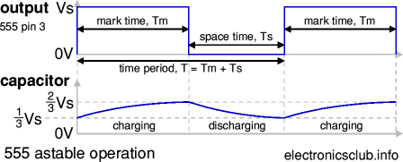
With the output high (+Vs) the capacitor C1 is charged by current flowing through R1 and R2.
The threshold and trigger inputs monitor the capacitor voltage and when it reaches 2/3Vs (threshold voltage) the output becomes low and the discharge pin is connected to 0V.
The capacitor now discharges with current flowing through R2 into the discharge pin. When the voltage falls to 1/3Vs (trigger voltage) the output becomes high again and the discharge pin is disconnected, allowing the capacitor to start charging again.
This cycle repeats continuously unless the reset input is connected to 0V which forces the output low while reset is 0V.
An astable can be used to provide the clock signal for circuits such as counters.
A low frequency astable (< 10Hz) can be used to flash an LED on and off, higher frequency flashes are too fast to be seen clearly. Driving a loudspeaker or piezo transducer with a low frequency of less than 20Hz will produce a series of 'clicks' (one for each low/high transition) and this can be used to make a simple metronome.
An audio frequency astable (20Hz to 20kHz) can be used to produce a sound from a loudspeaker or piezo transducer. The sound is suitable for buzzes and beeps. The natural (resonant) frequency of most piezo transducers is about 3kHz and this will make them produce a particularly loud sound.
Rapid Electronics: NE555 timer
Next page: 555 Monostable
Also see: 555 Timer | Bistable | Buffer
